The semiconductor industry is entering a defining phase.
Artificial intelligence is no longer just a workload running on advanced chips — it is fundamentally influencing how those chips are designed. As AI-driven applications demand higher performance, tighter power efficiency, and increasingly complex architectures, the pressure on verification, test, and implementation teams continues to intensify.
In this evolving landscape, design services must also adapt. The future will not be defined by larger teams or faster scripting alone, but by structured execution, clear risk visibility, and more predictable, AI-enabled engineering outcomes.
Design Execution Complexity Is Growing Faster Than Ever
As semiconductor technology continues to scale from mature nodes (65nm to 40nm) to mid-generation nodes (28nm, 16/14nm) and further into advanced nodes (12nm, 8nm, 7nm, 5nm and beyond), design execution complexity is increasing at an unprecedented pace.
Semiconductor design execution — spanning Design Verification (DV), Design for Test (DFT), Physical Design (PD), and signoff — has always required precise coordination across multiple engineering domains. However, with each node transition, constraints tighten and interactions become more complex, significantly amplifying execution challenges. Across both verification and implementation flows, teams must now navigate:
- Extremely tight timing margins at advanced nodes
- Congestion-driven ECO cycles during backend implementation
- Rapidly increasing DRC and LVS rule complexity
- Power integrity challenges and heightened IR-drop sensitivity
- Large-scale verification regressions with complex debug cycles
- Aggressive tapeout schedules across multi-team programs
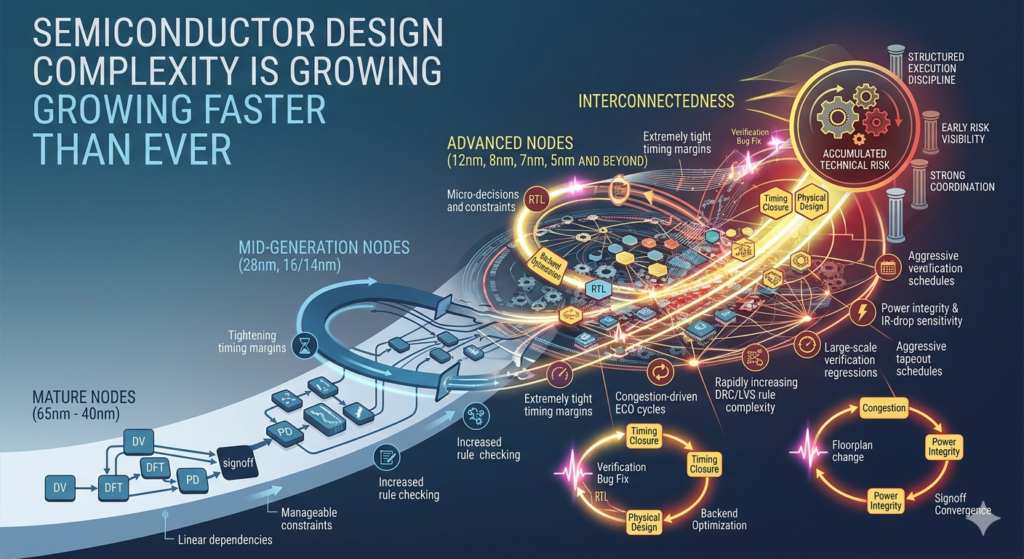
As a result, design execution is no longer just more complex — it is highly interconnected and sensitive to change. Even small modifications in one stage can propagate across the entire program. For example:
- A verification bug fix at RTL can impact timing closure downstream
- DFT insertion may introduce new timing paths affecting backend optimization
- Floorplan changes can influence congestion, power integrity, and signoff convergence
In this context, chip development is no longer about executing isolated tasks within the design flow. It is about managing accumulated technical risk across verification, implementation, and signoff stages.
Successful design programs, therefore, depend on structured execution discipline, early risk visibility, and strong coordination across DV, DFT, PD, and signoff teams.
The Limits of Traditional Design Service Models
Historically, semiconductor design services have relied on execution models centered around manual engineering workflows and iterative debugging cycles.
Across both verification and implementation stages, these approaches typically depend on:
- Manual analysis of large verification regression logs
- Repeated ECO iterations during backend implementation
- Experience-driven debugging of timing and design issues
- Resource scaling primarily through increased engineering headcount
This model proved effective when technology nodes were more forgiving and design schedules allowed greater flexibility. However, as semiconductor technology has scaled and SoC complexity has increased, these reactive approaches are becoming less effective in maintaining predictable execution.
Increasing Pressure Across the Design Flow
Modern semiconductor programs now operate under significantly tighter constraints and higher complexity. Across the design flow, teams must manage:
- Large-scale verification regressions generating extensive debug data
- Complex DFT insertion and scan integration requirements
- Tight timing margins during backend implementation
- Strict signoff criteria across multiple analysis domains
When issues emerge late in the design cycle, the impact can be substantial. Teams often encounter:
- Prolonged verification debug cycles
- Escalating ECO iterations during timing closure, including increased hold buffer insertion
- Compressed signoff validation windows
These factors can introduce instability into the overall program timeline and make execution outcomes less predictable.
Experience Alone Is No Longer Enough
Engineering expertise remains one of the most valuable assets in semiconductor development. However, as design data continues to grow in both volume and complexity, relying solely on manual analysis and experience-driven debugging is no longer sufficient.
Design teams are now required to interpret large volumes of:
- Simulation logs; Timing reports; DRC and LVS reports
- Power integrity and IR-drop analysis data
Extracting meaningful insights from this data manually can significantly slow engineering productivity and delay convergence toward tapeout.
The Need for Structured Execution Intelligence
As semiconductor design complexity continues to increase, successful programs require more than technical expertise alone. They require a more disciplined and structured approach to execution. This includes:
- Structured execution discipline
- Clear engineering visibility across design stages
- Early detection of emerging technical risks
As a result, the industry is gradually moving toward execution intelligence models — approaches that enhance engineering workflows through improved monitoring, structured analysis, and better decision support. These models enable teams to maintain stability across verification, implementation, and signoff phases, while improving overall program predictability.
The Evolution of the ODC Model
Traditionally, Offshore Development Center (ODC) models have focused on cost optimization and resource augmentation. However, as design complexity increases and execution risk becomes more critical, the role of ODCs is evolving. In the coming years, the ODC model will shift toward:
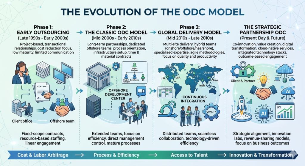
- Defined ownership of execution milestones
- Transparent and structured reporting frameworks
- Strong escalation discipline for risk management
- Data-driven progress tracking
- Enhanced execution visibility supported by AI
As a result, clients are increasingly prioritizing predictability and execution control over cost alone. The service partner of the future will not simply extend engineering capacity — it will play a critical role in strengthening execution discipline and improving overall program outcomes.
Asmicore’s Perspective: Design Services as a Risk-Control Discipline
At Asmicore Semiconductor, backend design is not viewed simply as implementation — it is treated as a structured risk-control discipline.
Modern SoC programs accumulate technical risk across multiple dimensions, including timing closure, congestion, power integrity, verification stability, and ECO convergence. Managing this complexity requires more than engineering expertise alone; it demands clear execution visibility and disciplined coordination across the entire design lifecycle.
We believe the future of backend services lies in combining structured execution practices with intelligent insight, enabling teams to move from reactive problem-solving to controlled and predictable convergence.
1. Defined Accountability Foundation
Clear ownership across design stages is essential. Well-defined scope boundaries, milestone governance, and structured escalation mechanisms help prevent hidden risk accumulation and ensure alignment across teams.
2. Execution Intelligence Integration
AI should be applied thoughtfully — not as a trend, but as a practical support layer. When used correctly, it enhances monitoring, summarizes complex data, and improves visibility across PD, DV, and DFT flows, enabling faster and more informed decision-making.
3. Predictable Tapeout Philosophy
Successful tapeout should not rely on last-minute firefighting. Instead, it should be the result of structured checkpoints, measurable progress indicators, and early detection of potential risks.
4. Human + AI Hybrid Model
AI is not a replacement for engineering expertise — it is an enabler. The combination of deep domain knowledge and structured intelligence leads to more stable, efficient, and controlled execution environments.
At Asmicore, the objective is not simply task completion — it is achieving controlled and predictable convergence toward signoff.
Toward Predictable Tapeout
In an AI-driven semiconductor industry, the true competitive advantage is shifting toward predictability, and that indicates ‘predictable timing closure, predictable verification stability, and predictable signoff readiness.’ Achieving this level of predictability requires more than scaling engineering teams. It requires continuous visibility into execution across the entire design lifecycle.
Timing trends must be observable across implementation iterations. Verification regressions should reveal meaningful patterns rather than isolated failures. Implementation convergence should be actively monitored, not discovered late in the schedule. This is where execution intelligence becomes critical.
At Asmicore, we see AI-assisted platforms as a means to introduce structured visibility into engineering workflows — enabling teams to identify trends, detect risks earlier, and make informed decisions throughout the design cycle. Instead of reacting to issues late, teams can move toward a model of controlled and measurable convergence toward tapeout.
As a result, backend design services are evolving from execution vendors into long-term program partners, focused on reducing uncertainty and strengthening execution control.
Final Thoughts
The semiconductor landscape continues to evolve rapidly, but the core objective remains unchanged, which is to deliver high-quality silicon on schedule. What is evolving is how that goal is achieved. The future of backend design services lies at the intersection of:
- Deep technical expertise
- Structured execution governance
- AI-driven execution intelligence
Organizations that successfully align these elements will define the next generation of semiconductor delivery models. At Asmicore, this evolution is not about replacing engineers with AI — it is about empowering engineering teams with structured intelligence, transforming complex design programs into predictable, scalable, and sustainable tapeout outcomes — even in increasingly complex design environments.